Electronic Devices — DPP 2

20 NEET questions from Electronic Devices, with answers and explanations. Attempt it as a timed test to get scoring, accuracy breakdown and mistake tracking.

Attempt this test free 20 questions · 30 minutes · +80 marks
1
Which of the following diode is reverse biased:-
  1. A
  2. B
  3. C
  4. D PSE036
Show answer

Correct answer: C
2
In a unbias p-n junction :-
  1. A high potential is at n side and low potential is at p side.
  2. B high potential is at p side and low potential is at n side.
  3. C p and n both are at same potential.
  4. D undetermined.
Show answer

Correct answer: A

3
The resistance of a reverse biased pn junction diode is about :-
  1. A 1 ohm
  2. B $10 ^ { 2 } \mathrm { ohm }$
  3. C $10 ^ { 3 } \mathrm { ohm }$
  4. D $10 ^ { 6 }$ ohm
Show answer

Correct answer: D

4
In germanium crystal, the forbidden energy gap in joule is :-
  1. A $1.6 \times 10 ^ { - 19 }$
  2. B zero
  3. C $1.12 \times 10 ^ { - 19 }$
  4. D $1.76 \times 10 ^ { - 19 }$
Show answer

Correct answer: C

5
In a P-N Junction diode not connected to any circuit
  1. A potential is the same everywhere.
  2. B the P - type side is at a higher potential than the N - type side.
  3. C there is an electric field at the junction directed from the N-type side to the P-type side.
  4. D there is an electric field at the junction directed from the P-type side to the N-type side.
Show answer

Correct answer: C

6
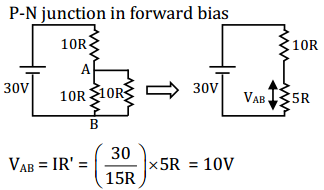
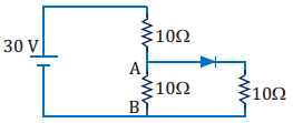
Find V$_{AB}$:-
Electronic Devices – NEET-13967
  1. A 10 V
  2. B 20 V
  3. C 30 V
  4. D none
Show answer & explanation

Correct answer: A

Electronic Devices – NEET-13967
7
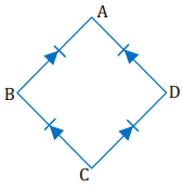
For the given circuit shown in fig, to act as a full-wave rectifier:- a.c. input should be connected across ___________ and ___________ the d.c. output would appear across ___________ and ___________
Electronic Devices – NEET-13978
  1. A A, C, B, D
  2. B B, D, A, C
  3. C A, B, C, D
  4. D C, A, D, B
Show answer

Correct answer: B

8
The minority current in a p-n junction is :-
  1. A from the n-side to the p-side
  2. B from the p-side to the n-side
  3. C from the n-side to the p-side if the junction is forward-biased and in the opposite direction if it is reverse biased.
  4. D from the p-side to the n-side if the junction is forward-biased and in the opposite direction if it is reverse biased
Show answer

Correct answer: A

9
On increasing the temperature the specific resistance of a semiconductor :-
  1. A increases
  2. B decreases
  3. C does not change
  4. D first decreases and then increases
Show answer

Correct answer: B

10
Depletion layer in p-n junction region is caused by
  1. A drift holes
  2. B diffusion of free carriers
  3. C migration of impurity ions
  4. D drift of electrons
Show answer

Correct answer: B

11
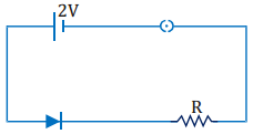
A 2 V battery forward biases a diode however there is a drop of 0.5 V across the diode which is independent of current. Also a current greater then 10 mA produces large joule loss and damages diode. If diode is to be operated at 5 mA, the series resistance to be put is :-
Electronic Devices – NEET-13965
  1. A 3 kΩ
  2. B 300 kΩ
  3. C 300 Ω
  4. D 200 kΩ
Show answer & explanation

Correct answer: C

When P-N junction is operated at 5 mA
(2 – 0.5) = 5 × 10$^{–3}$ × R
R = 300 Ω
12
What is the energy gap in Si semiconductor?
  1. A 4.4 eV
  2. B 0.3 eV
  3. C 0.7 eV
  4. D 1.1 eV
Show answer

Correct answer: D

13
The width of depletion region in a p-n junction diode
  1. A increases when reverse bias is applied.
  2. B increases when a forward bias is applied.
  3. C decreases when a reverse bias is applied.
  4. D remains the same irrespective of the bias voltage.
Show answer

Correct answer: A

14
The majority current in a p-n junction is :-
  1. A from the n-side to the p-side
  2. B from the p-side to the n-side
  3. C from the n-side to the p-side if the junction is forward-biased and in the opposite direction if it is reverse biased
  4. D from the p-side to the n-side if the junction is forward-biased and in the opposite direction if it is reverse biased
Show answer

Correct answer: B

15
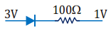
Assuming that the junction diode is ideal then the current through the diode is:-
Electronic Devices – NEET-13968
  1. A 200 mA
  2. B 20 mA
  3. C 2 mA
  4. D zero
Show answer & explanation

Correct answer: B

$I=\frac{3 V-1 V}{100 \Omega}=20 \mathrm{~mA}$
16
In a p-n junction the depletion layer of thickness $10 ^ { - 6 } \mathrm {~m}$ has potential across it is 0.1 V. The average electric field is (V/m) :-
  1. A $10 ^ { 7 }$
  2. B $10 ^ { - 6 }$
  3. C $10 ^ { 5 }$
  4. D $10 ^ { - 5 }$
Show answer & explanation

Correct answer: C

Electric field $=\frac{\mathrm{V}}{\mathrm{d}}=\frac{0.1}{10^{-6}}=10^{5}(\mathrm{~V} / \mathrm{m})$
17
Correct statement for diode is :-
  1. A in full wave rectifier both diodes work alternatively.
  2. B in full wave rectifier both diodes work simultaneously.
  3. C efficiency of full wave rectifier and half wave rectifier is same.
  4. D full wave rectifier in bidirectional.
Show answer

Correct answer: A

18
When we convert pure semiconductor into N type the number of hole :-
  1. A Increases
  2. B Decreases
  3. C Remains constant
  4. D None
Show answer

Correct answer: B

19
When a junction diode is reverse biased, the flow of current across the junction is mainly due to :-
  1. A diffusion of charges
  2. B depends upon the nature of material
  3. C drift of charges
  4. D both drift and diffusion of charges
Show answer

Correct answer: C

20
In p-n junction at the near at junction there are :-
  1. A positive Ions
  2. B negative Ions
  3. C positive and negative Ions
  4. D electrons and holes
Show answer

Correct answer: C

Attempt this as a timed test

Reading answers is not the same as sitting the paper. Attempt it timed and you get your score, per-question timing, and the mistakes tracked for revision.

Start free

More Electronic Devices tests

All Electronic Devices tests →